
Updated AVCX LCD Controller

Graphics LCDs are now available for hobbyists, both B/W and color, but a lot of them have no controller, meaning they have to be provided with constantly repeating line data. This is a full-time job, even for AVRs. On top of that, the information to be displayed on the screen has to be stored in RAM memory, and requires a lot more than the small amount of RAM available on most microcontrollers.
Here are some numbers for the Sony ACX705AKM color LCD. This is a very nice LCD, providing 160 lines of 240 pixels, each pixel consisting of 9 color bits (3 Red, 3 Green and 3 Blue). Even simplifying the color depth to 8 bits (1 byte), still requires 160 x 240 = 38,400 bytes, way more than available on an AVR.
To get a refresh rate of 60 Hz, the LCD needs to be fed 60 * 240 * 160 bytes per second (2,304,000 bytes per second), one byte every 434 nSeconds, over and over again. Because of overscan, the actual rate is higher. Then there is the need to get the data to be displayed from somewhere, let alone doing actual work.
All in all, quite the challenge. Luckily for us, a very elegant solution has been designed by Michal S., the winner of the Circuit Celler AVR 2004 Design Contest. He uses 2 AVRs, and Atmega8515 and an Atmega128, plus 128KB external SRAM to drive the LCD, while still leaving enough time to accept data to be displayed over a serial link. He calls it the AVCX controller.
Hardware
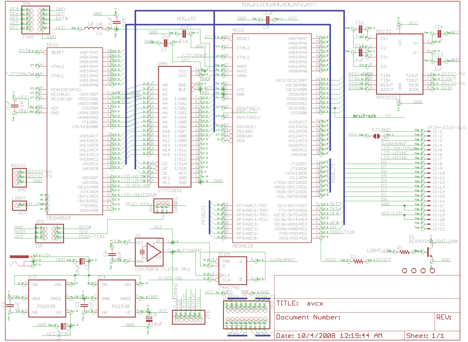
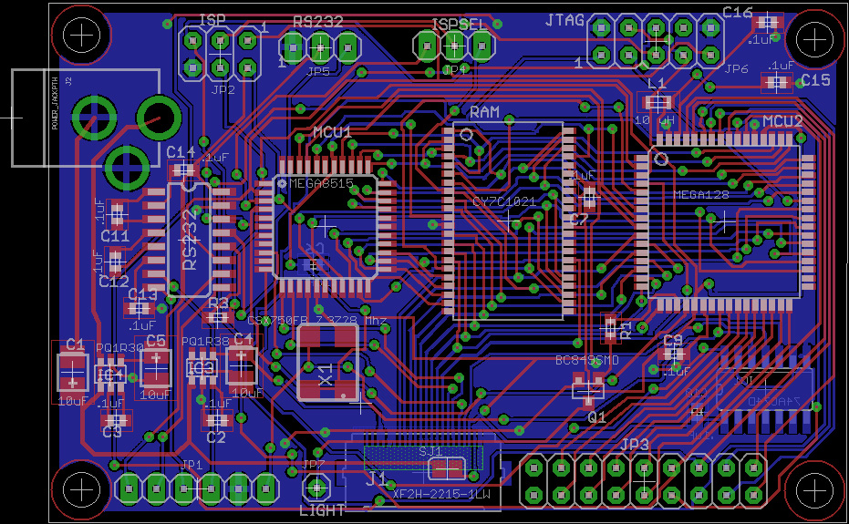
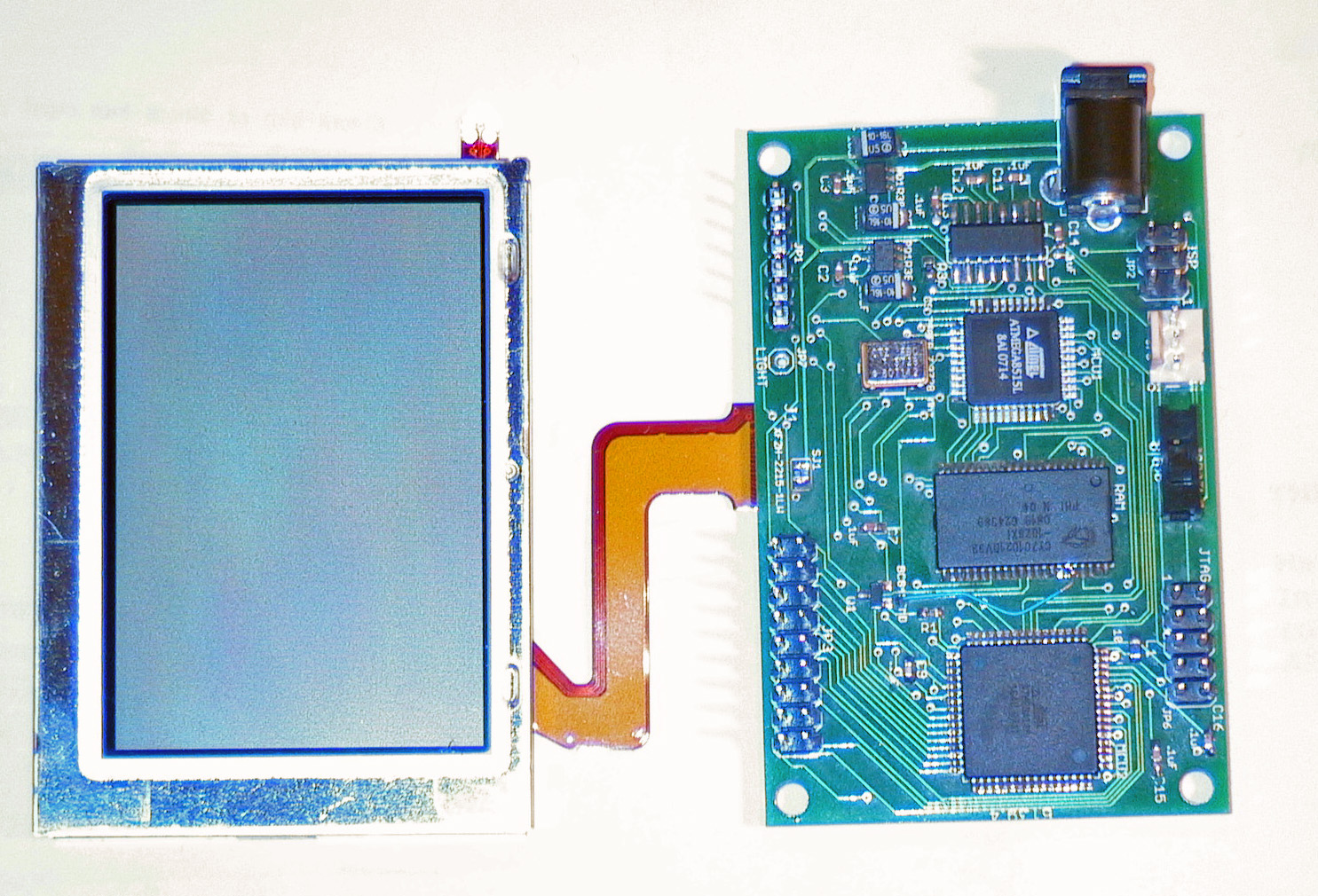
The Sony ACX705AKM LCD, used by Michal, is available at The Electronic Goldmine for less than $20 (though their shipping is very expensive), which makes it tempting to build this design. The only problem is the fact that his design is all surface mount, for many good reasons incl. the necessary 0.5mm pitch FFC connector to the LCD. Pictures of the board, the schematics and the traces are all available, but not actual design files to reproduce the PCB shown.
So I took it upon me to create the PCB using the Eagle PCB design package, adding some conveniences in the process. It turns out that the schematics doesn't quite match the published PCB images, so I had to tape the PCB front and back images back to back and use a needle poking through the paper to follow some of the traces not present in the schematics. As far as I can see, the changes are related to the LCD backlight and are not important for the overall design.
I made the board a little bigger and added connectors so there is no need for an auxiliary board. I also added a JTAG connector to debug the Atmega128. Programming both AVRs is possible using the 6-pin ISP connector and the ISPSEL switch (left for Atmega8515, right for Atmega128.) I found programming the Atmega128 with this ISP setup not reliable (long lines?) but the JTAG interface works like a charm.
Here are the Schematics and PCB Design Images:
The Eagle design files can be downloaded here:
Using this controller isn't all that easy because of the unusual graphics color depth of 9 bits. I was hoping to use the Windows version of the netpbm suite of tools (graphics utilities for Linux) to manipulate the graphics files to get the desired file format but was unsuccessful. The program to do the actual color depth remapping (name?) kept on crashing.
In the end I used photoshop to create a bitmap file with the correct resolution (240 x 160) and a 16-bit color depth but with the unusual X4R4G4B4 option (so actually 12 bits color depth) and wrote a separate program to send data to the AVCX controller over the serial port; when this program sends the bitmap, it just removes the lowest color bit. This is sub-optimal since a better color result can possibly be achieved by other techniques like dithering, but it works and I'm not that interested in graphics manipulation. I'd love to hear about tools that generate good 9 bit (3R3G3B) color depth files.
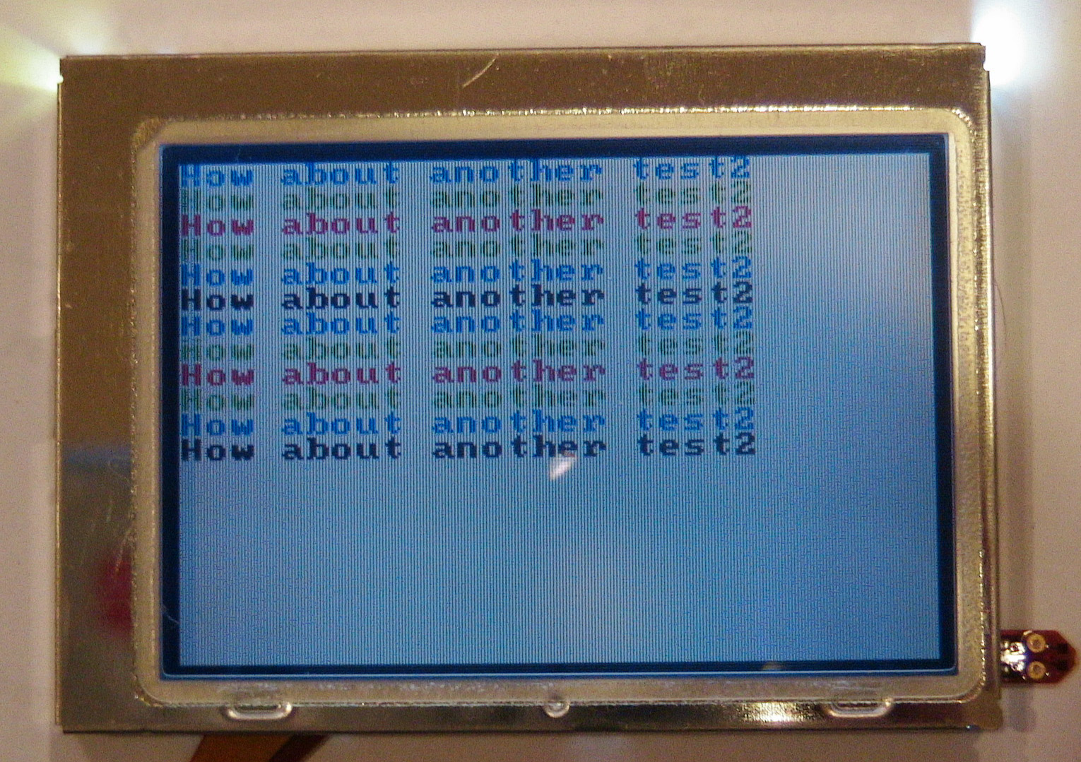
Here is what the result looks like:
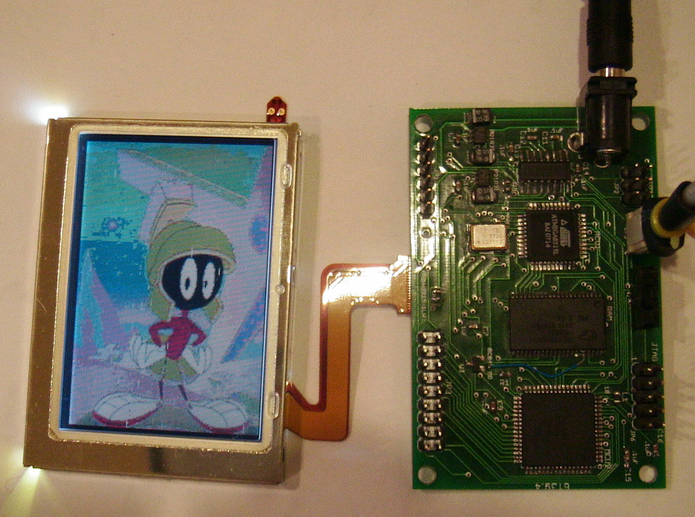
Note: if you decide to buy this LCD from The Electronic Goldmine, consider NOT buying the matching Molex 22-pin connector they sell for $3.00. The Omron XF2H-2215-1LW connector actually works better (it has contacts on both sides) and is only $0.89 at Digikey. Enjoy soldering a 0.5mm pitch connector!
Software
After building the hardware, I used the source code as included with the Circuit Cellar 2004 AVR Design Contest and with a minor bug fix, it worked. After some more research I found that the software actually didn't work as documented in the project files: theory didn't quite match reality. The problem was that there isn't enough time for MCU2 to update the shared memory in the allotted time period. The original author fixed this by including in hardware a control line to "freeze" the pixel clock, adding wait states at the end of each horizontal scan line. To be more precise, the horizontal scan timing was doubled, reducing the LCD refresh rate to about 30 Hz. It still gave a good picture though.
In general, the only time MCU2 can access the shared video memory is between INT6 and INT7 events (the RAM window). Incoming graphics commands are stored in a buffer which is processed during the RAM window, when it is safe to write to the video memory.
Issues were:
The incoming bytes buffer was only 256 bytes but the CLRSCR command for example takes 57 mSecs to execute, which equates to 663 incoming bytes at 115,200 bps. A lot of these bytes could be discarded. The full bitmap command expect 76,800 data bytes. With multi-byte commands, the state machine gets out of sync when incoming data must be discarded.
The graphics command processing during INT6 was not always completed before INT7 occurred, requiring a clever and tricky recovery mechanism to make sure the previous processing was completed on the next INT6. This mechanism required that no functions were called while doing graphic commands processing.
While graphics processing occurred during the INT6 ISR (the RAM window), no incoming bytes were accepted.
the RAM window is fairly long at the end of each screen. From lines 160 to 200, the RAM window is open all the time because this is "overscan" time. Even though the HSYNC signal is still properly issued, no data bytes are used by the LCD. In the original design, the RAM window was closed at line 185, probably because too many serial input bytes were lost. (the serial input was disabled during the RAM window in the original design)
To fix this low refresh rate, I completely redesigned the runtime design of MCU2.
The new design uses a 2K input buffer, plenty for the most demanding input. It also accepts incoming characters at all times. There are a few short moments where interrupts are disabled, mostly to ensure atomic operations on 16 bit pointers or when toggling the memory controls.
Graphics processing is now done in the forever loop, not in an ISR. The forever loop gets interrupted when an INT7 occurs. The INT7 ISR releases the memory bus, sets the state to FROZEN, enables interrupts and waits until the state changes to UNFREEZE. This state change occurs when INT6 hits. INT6 does nothing but changing the state. INT7 grabs the memory bus again and finishes, allowing the forever loop to continue graphics processing at the point it was interrupted. In summary, when the forever loops runs, it is safe to access the video memory. When it is not safe, the code loops inside the INT7 ISR. Incoming bytes are accepted at all times. The performance of MCU2, specially wrt incoming bytes, is now guaranteed, independent of the specific timing of INT6 and INT7 (as long as they alternate)
Well almost. There were also screen artifacts at the beginning of each line when MCU2 was accepting incoming data. These artifacts were caused by the fact the MCU2 didn't release the memory bus fast enough (the INT7 interrupt could occur while inside the Serial-in ISR which needs to finish before the INT7 ISR is executed, see below) causing bus contention. This was fixed by sending the RAM_STOP signal from MCU1 to MCU2 earlier (from Dot clock 262 to Dot clock 252). This however leaves only 8 dot clocks (16 cycles) for MCU2 to access the memory, which is not enough, causing even a 2K input buffer to overflow. So some freeze (12 uSecs, value = 15, original value was 100) is still present.
During the VSYNC period, the RAM window is now closed at line 200, allowing for a longer RAM window.
Part of the reason why INT7 is slow to respond on MCU2 is the fact that Serial-in interrupts are always on. When the INT7 interrupt occurs while a serial input is active, the INT7 interrupt is pended and won't get triggered until the serial input interrupt is completed. For this reason, the Serial Input ISR processing must be as short as possible.
The redesign resulted in an LCD refresh rate of 66.6 Hz, double the original design, with little, if any, serial input rate limitations.
The Sony LCD supports a 9-bit color depth per pixel. 9 bits is an awkward number for an 8 bit processor. To send a complete bitmap over the serial port in 9 bits, the original design used 2 bytes per pixel, for a total of 76,800 bytes. Even at 115200 bps, this still takes over 6 seconds. Therefore I added a "Short bitmap" command, which only sends 8 bits, ignoring the lowest BLUE bit. Sending the short bitmap still takes 3.3 seconds.
Other observations:
It would be nice to have a way to reset the Graphics Commands parser, There are multi-byte commands plus the bitmaps, which expect 38,400 or 76,800 bytes. Once the parser gets out of sync, it may gobble the next 76,800 input bytes as it expects bitmap data. Adding a reset on time-out is one possibility.
The current design relies on registers X and Y to be dedicated to the Serial Input buffer (to make the Serial-in ISR as short as possible), which makes it difficult to convert the code to C. I have tried to use memory based pointers but this results in memory bus contention at the beginning of the scan lines when serial data are coming in to MCU2, because it can take too long for MCU2 to respond to the INT7 request from MCU1 (Serial-in ISR is too slow). If this program needs to be converted to C, the timing of INT7 in MCU1 must be advanced, at least to DotClock 248. The freeze window may have to be extended too in that case.
The updated source code plus a data sending application running on a PC can be downloaded here:
This is what the readme.txt file says:
Source files for Michal's AVCX project which is described here:
The source files for the AVR processors originate from the Circuit Cellar 2004 AVR Design Contest and are used with permission from Circuit Cellar.
MCU1: Atmega8515 AVR, the master CPU which drives the LCD and controls MCU2
MCU2: Atmega128. This CPU updates the shared memory with data coming from the Serial Interface
AVCXAccess: Visual C++ 9.00 Express Edition application sending text and a bitmap to the AVCX controller. This is a quick and dirty application, using a lot of code borrowed from other sample applications. You will have to change the serial port for your own situation.
Pict_01.BMP. This is an image created with Adobe Photoshop elements 3.0. It has 160 lines of 240 chars each and a colordepth of 12 pixels (X4 R4 G4 B4). The AVCXAccess application only uses the upper 3 bits of each color.
For suggestions and corrections, please contact me at:
![]()
Please remember, this project was originally designed and implemented by Michal Sieluzycki, now deceased, who deserves all the credit. I only implemented the PCB design and redid some of the software for MCU2.
![]()
![]()
![]()
![]()