Full speed AVR based Graphics LCD Controller
for Epson P300013100 display
Graphics LCDs are now available for hobbyists, both B/W and color, but a lot of them have no controller, meaning they have to be provided with constantly repeating line data. This is a full-time job, even for AVRs. On top of that, the information to be displayed on the screen has to be stored in RAM memory, and requires a lot more than the small amount of RAM available on most microcontrollers. Lucky for us, not for this particular LCD.
The Epson P300013100 is a monochrome LCD display with a resolution of 600 x 200 pixels and NO controller. It has a 4 bit (nibble) data interface, the usual DotClk, HSYNC, VSYNC and M(AC) lines, unusual YSHIFT and X Enable lines plus a Display Enable line. Power requirements are +5V (Vcc) and -13V to -20V LCD Bias(Vee). This LCD has an unusual 20 pin connector but this connector can be replaced with a standard 0.1" 20 pin header. A 20-wire IDC cable can be used with such a header.
The detective work of figuring out the function of each pin and how to drive these pins was done by kcbartsch. His research showed that the display is internally organized as 1280 x 100, 100 lines of 1280 pixels each, where the second half of each line (pixels 640..1279) is shown on the bottom half of the display.
The "M" input is an oscillating input needed to prevent the LCD crystals from being operated in DC mode. It needs to alternate between GND and Vcc constantly to prevent damage to the LCD crystals. This means that, once the Enable line is set High, the timing lines need to be constantly toggled to prevent damage when Vee is connected (-15V LCD Bias voltage). This means that no ICE debugging can be done while Vee is connected. Unplug the Vee line when using the Jtagice mkII! There is a 2-pin header with shunt in the lower right corner of the PCB for that purpose.
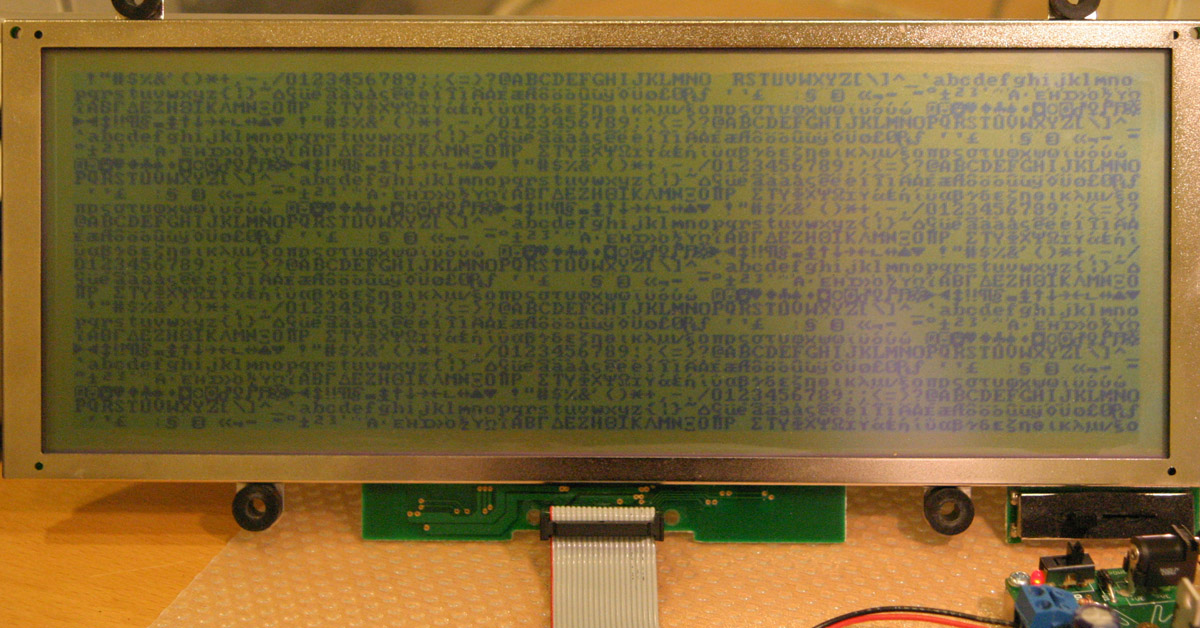
This display has no backlight, which makes viewing the images more difficult; it also makes taking pictures or video very difficult and the pictures and video on this page are not of the best quality.
The controller design.
The task of an LCD controller is to send one line of data to the LCD, toggling the DOTCLK line for every nibble, then toggle the HSYNC and YSHIFT signals, which forces the LCD to show this one line on the screen and to prepare for the next line of data. Once all lines are sent, the VSYNC signal needs to be toggled, indicating that the LCD needs to start at the top of the screen for the next line of data. This LCD also requires that the X Enable line is pulled high whenever the data need to be moved to the next SED1180 chip (an SED1180 is a 64-segment driver; there are 20 of these on the LCD). Doing this fast enough will create the illusion to our eyes of a stable image. It is the same principle as the raster scan method used in CRT video display and TV. At the same time, the controller must provide an interface to the outside world to allow useful information to be sent to the display, so that there is something to show (the user interface).
The internal resolution of this display is 1280 horizontal by 100 vertical. Since the horizontal input is done 4 bits at a time, we need to toggle 1280 / 4 = 320 nibbles per line. To do one frame, we need 320 * 100 = 32,000 nibbles, or 16,000 bytes
This LCD does not require any overscan. Overscan is a left over from the old CRT designs, where the controller needs to provide extra time between lines and frames to allow the electron beam to move to the next location (beginning of next line or top of screen). Some other LCDs, for example the Sony ACX705AKM as used in the AVCX project, do require this overscan (according to the datasheet), which makes it harder for one microcontroller to do all the work (though not impossible).
To achieve a refresh rate of 60 Hz (progressive scan), we need to clock 60 * 32,000 = 1,920,000 nibbles per second. In this design, each nibble takes 5 cycles, which includes the DOTCLK toggling. There is also about 70 cycles overhead for each line (register setup, Hsync, sometimes Vsync, Enable). The total number of cycles required to refresh this display is thus 5 * 1,920,000 + 70 * (100 * 60) = 10,020,000 per second. For an AVR running at 20 Mhz, this means it's busy about 50% of the time doing refreshes, leaving 50% for other tasks, mainly to update the display memory based on external graphics commands from the user interface.
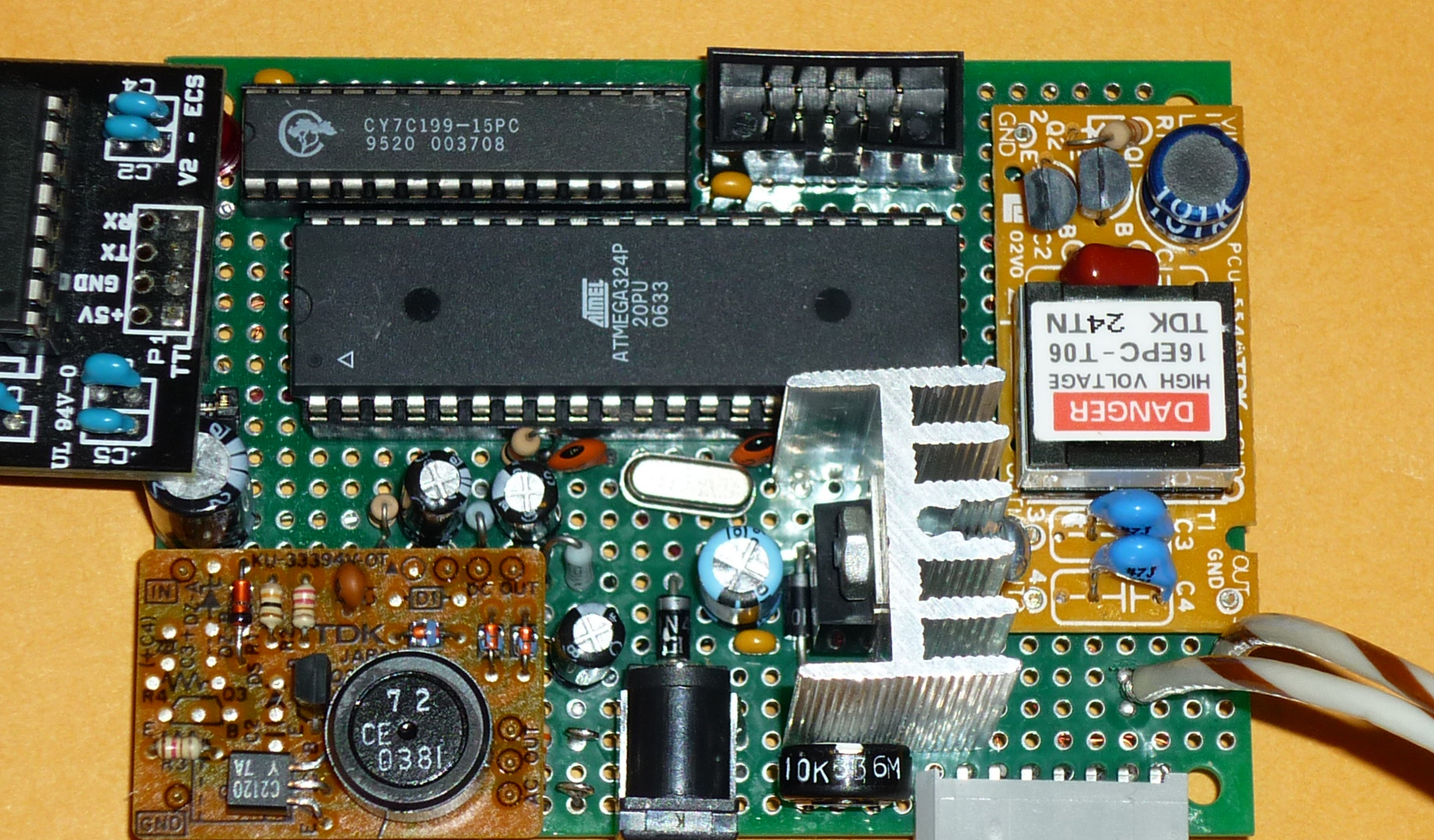
As mentioned, one frame requires 32,000 nibbles of memory, which equates to 16,000 bytes. Most AVRs don't have that much memory but one does, the Atmega1284p, which has 16,384 bytes of internal SRAM, just enough for our purposes. Therefore, this controller does not require an external RAM chip to store the bitmap (unlike previous LCD controllers I built, which require an external RAM chip).
The AVR assembly code to refresh 2 nibbles of the Epson LCD looks like this:
|
.macro |
UpdateColumns | |
|
ld |
r16,Z+ | ; get next byte |
|
swap |
r16 | ; upper nibble first |
|
out |
DOTCLK_PORT,PORTDCLKON | ; same as sbi DOTCLK |
|
out |
SRAMDATAO,r16 | ; nibble to LCD |
|
out |
DOTCLK_PORT,PORTDCLKOFF | ; same as cbi DOTCLK |
|
swap |
r16 | ; lower nibble |
|
out |
DOTCLK_PORT,PORTDCLKON | ; same as sbi DOTCLK |
|
out |
SRAMDATAO,r16 | ; nibble to LCD |
|
out |
DOTCLK_PORT,PORTDCLKOFF | ; same as cbi DOTCLK |
|
.endm |
PORTDCLKON and PORTDCLKOFF are register that have been preloaded with the current value of the DOTCLK_PORT, modified to either CLR or SET the DOTCLK bit. This technique avoids the use of the sbi and cbi instructions which each are 2 cycles, as opposed to the out instruction which is just 1 cycle. The total is 10 cycles for 2 nibbles, 5 cycles per nibble.
This macro is executed 8 times per SED1180, inside a loop for the 20 SED1180 chips on the LCD, for a total of 2 * 8 * 20 = 320 nibbles per line, 100 lines per screen, which is the internal 1280 x 100 architecture.
The refresh is done using Timer0, which is executed every 166.4 microseconds (6,009 Hz). At 100 lines per frame, we get 6,009 / 100 = 60 frames per second, producing a rock solid image. To optimize the refresh cycle count, the Timer0 ISR is written in AVR assembly, but everything else is written in C (Winavr).
Access to the internal SRAM inside the AVR is very simple. The memory buffer is declared as:
uint8 FrameBuffer[PHYS_LINES*BYTES_PER_LINE];
PHYS_LINES equals 100;
BYTES_PER_LINE equals 160;
Because the FrameBuffer is very large (16,000) bytes, there are only 384 SRAM bytes left, which includes stack space. This rules out a large input buffer for the interrupt driven Serial handler. My DMF50840 design uses a 512 bytes input buffer, which works fine, meaning the input buffer never overflows. In this design, we only can afford a much smaller buffer, 128 bytes at the most, which will in all likelihood overflow when sending data at 115,200 bps. Therefore I added software flow control using the ^S, ^Q convention. Now, if the input buffer is 3/4 full, the controller will send an XOFF (^S) code to the sender, telling it to stop sending. When the buffer becomes less than 1/4 full, the controller will send an XON (^Q) code, telling the sender it's ok to send data again. Note that this technique works only if the sender only expects ascii characters from the controller (like status messages), so that the sender can interpret these XOFF and XON binary codes properly. The sender cannot use flow control because this controller, which is the receiver, expects binary data (the enhanced AVCX graphics protocol) and cannot distinguish between AVCX data and the XOFF/XON codes. In that case, hardware control lines would be needed to add flow control.
Please note that the XOFF/XON software flow control protocol does not work well with the FTDI USB to Serial converter default settings. This protocol requires that the XOFF byte is processed immediately by the PC so that sending more data is stopped ASAP to prevent buffer overflow on the controller. Unfortunately, the FTDI converter has a default "latency time" of 16 ms before databytes are transferred to the PC. Good for efficiency, bad for flow control. This "latency time" can be changed in the properties of the USB Serial port in the Device Manager (Windows): Port Settings, Advanced, under "BM Options"; change the "Latency Timer (msec)" value to 1. For more information on this issue, see FTDI application note TN_103.
The rest of the controller consists of this interrupt driven Serial handler with flow control, a general purpose TC1 timer used for bookkeeping purposes and the main forever loop which pulls graphic command data from the input buffer, parses them and updates the internal AVR memory accordingly. The controller currently is capable of displaying text (8 x 8 font), monochrome images, arbitrary pixels and has DrawLine and DrawCircle primitives. The graphic command language is based on the AVCX command language. A PC based application, called AVCXaccess, is used to send graphic commands over the serial port to the controller at 115,200 bps. This application uses overlapped Serial port I/O so that both output and input can be handled simultaneously.
The Enhanced AVCX graphics command language is a byte stream of data, where most commands require more than 1 byte. Losing a byte will therefore disrupt the synchronization between the controller and the PC. A timeout mechanism is present to reset the graphics controller if no input has been received for 5 seconds. This controller is a simplification of previous controllers I built, the DMF50840 controller and the AVCX project (based on another design). That AVCX project uses 2 separate AVRs, is surface mount on a dedicated PCB and is all written in AVR assembly language. The DMF-50840 controller uses a 40-pin DIP AVR (Atmega324p) plus a 28 pin DIP SRAM chip, both thru-hole, and is mostly written in C. This Epson P300013100 controller uses just one 40-pin DIP AVR (Atmega1284p) and is even easier to implement and modify.
The firmware of this controller also has a built-in analog clock. The clock face uses 200 x 200 pixels, left aligned at an offset of 20 pixels, leaving a pane of 420 x 200 pixels on the right side for other uses. The Enhanced AVCX graphics command language contains command to control the clock. No activity (meaning no incoming graphic control commands) for 1 minutes will also turn on the clock, as a screen saver.
The AVCX test program uses the same bitmaps as used for the DMF50840 graphics LCD. These bitmaps are 320 horizontal by 240 vertical. Since there are only 200 lines on this Epson LCD, the first 20 and the last 20 lines of each bitmap are unused. Since there are twice as many horizontal pixels (640) on this Epson LCD, 2 of these bitmaps will fit on the screen and the AVCX test program makes use of that.
The initial version of this controller was built using an STK600 and worked reliably. The current dedicated PCB was built using point to point wiring on the bottom side of the PCB using Chan's magnet wire technique. The components on the left side of the picture form a negative voltage generator (-15V) using the MC34063 controller, as shown here. The value of resistor R4 is 5K, the value of R2 is 4.7 KOhm. The current design uses an external 5V supply and a plug-in RS232 level converter board.
Here are the connections:
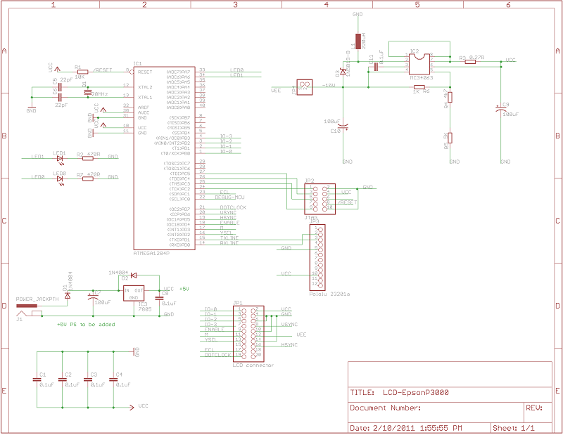
Atmega1284p connected to LCD:
PB0..PB3: Data bits 0..3
PD2: YSCL
PD3: M (AC)
PD4: LCD Enable
PD5: HSYNC
PD6: VSYNC
PD7: DOTCLOCK
PC1: ECL
Atmega1284p other:
PD0..PD1: Serial Interface to PC
PA6..PA7: Leds
PC0: Debug MCU
PC2..PC5: JTAG interface
LCD connector:
1..4: Data0..Data3
5: LCD Enable (PD4)
6: M (AC) (PD3)
7: YSCL (PD2)
8: n.c.
9: ECL (PC1)
10: DOTCLK (PD7)
11: Vcc (+5V)
12-13: Vss (GND)
14: VSYNC (PD6)
15: Vss (GND)
16: Vee (LCD Bias, -15V)
17: Vss (GND)
18: HSYNC (PD5)
19..20: n.c.
The 20-pin header on the LCD (LCD connector) uses an unusual numbering scheme. This header is located below the LCD screen, in the middle. Looking at it directly, the pins are numbered as follows:
__________20-pin LCD header___________
11 12 13 14 15 16 17 18 19 20
1 2 3 4 5 6 7 8 9 10
Pin1 is the left most pin on the bottom row. Pin11 is the left most pin on the top row.
Please note that the Atmega1284p fuse needs to be set to Full Swing External Crystal to operate reliably (I've learned that the hard way)
The user interface is currently driven by a demo application running on a PC ("AVCXAccess"). Communication with a PC requires the use of an RS-232 level converter. I used an external plug-in board for this. It is possible to use an FT232RL based USB-Serial adapter, however I found that such an adapter cannot be reliably used at speeds over 57600 baud.
Since development of the software for this controller is part of the fun, I wanted to have the ability to use the JTAGICE mkII hardware debugger. This requires that 4 pins (PC2..PC5) are reserved. Other enhancements to this controller are possible. For example, an SPI interface would make the user communication faster. Driving this controller from another AVR board will be one of the next projects. It should be possible to run the serial interface at +5V levels (no level conversion) and at much higher speeds.
The PC based application "AVCXAccess" is a demonstration program on how to send graphics commands and data to the LCD-EpsonP300013100 controller. The default is 115,200 at COM2 but is accepts 2 optional command line arguments for the COM port and the baudrate. Note that to change the baudrate, the controller software also has to be updated. A release build is included in the archive. The program will look for various bitmaps in the CURRENT directory so it needs to be started in the AVCXaccess directory like this: "Release\AVCXaccess.exe 1"; the optional '1' indicates that COM1: needs to be used.
Here are the Schematics:
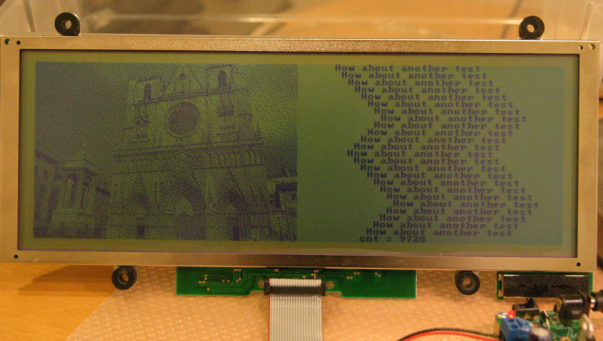
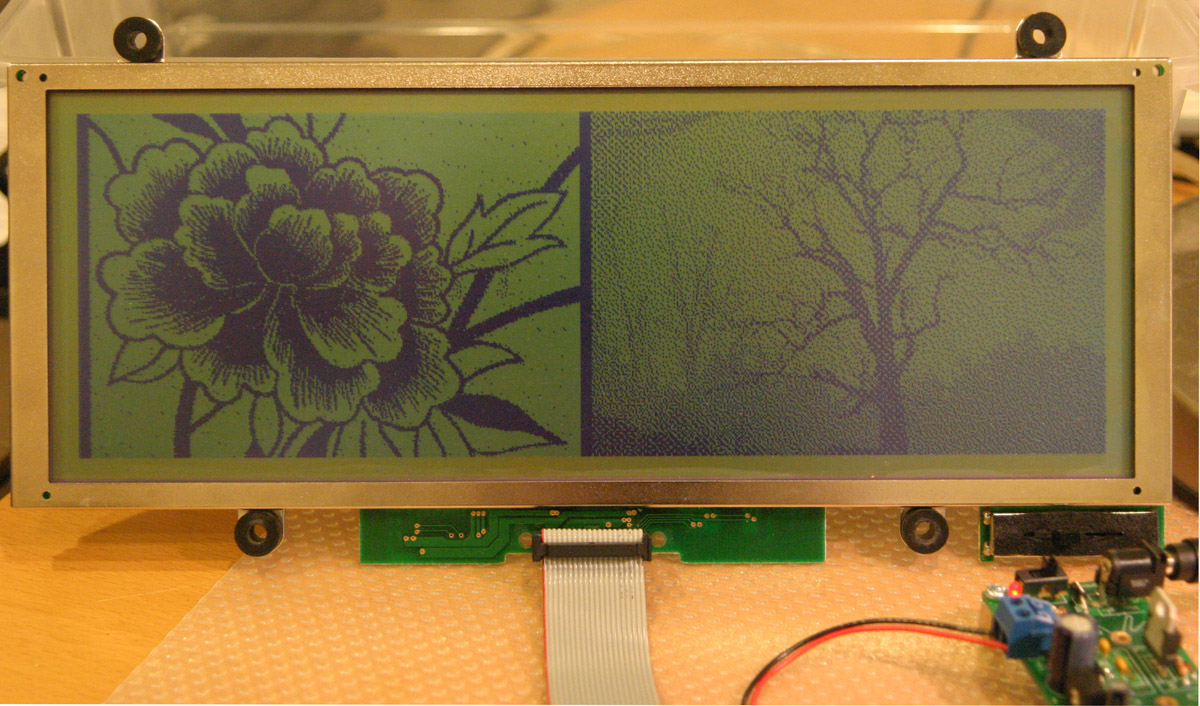
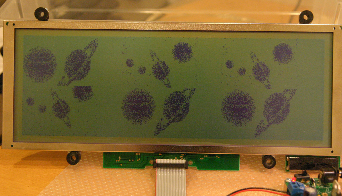
Here is what the result looks like:
.JPG)
|
|
|
|
|
|
|
|
Watch a video here. Unfortunately, the video quality is terrible due to the lack of a backlight:
Software
The WinAVR source code plus the AVCXaccess demo application sending graphic commands and data, running on a Windows PC, can be downloaded here:
For suggestions and corrections, please contact me at:
![]()
![]()
![]()
![]()
![]()
.JPG)